Thermal Laser Stimulation - TLS
The thermal laser stimulation bench is an optical microscope which enables to focus with precision, a PDM+ laser source (Pulse-on-Demand Module) at 1420 nm. Used through the back side of electronic components, the laser beam warms the sample locally and allows to extract and read out data in a memory according to the current consumption of the transistors.
Product reference: TLS laser bench
A side-channel technique
The aim of the thermal laser stimulation bench is to use the laser to warm strategic areas on the back side of the integrated circuits (SRAM, BBRAM, etc.). Depending on the power consumption of the transistors under the effect of the laser, it is possible to extract data from the memories. The aim of this technique is to help to secure integrated circuits.
A dedicated bench or a functionality added to a fault injection bench
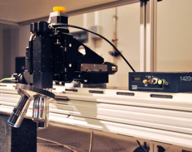
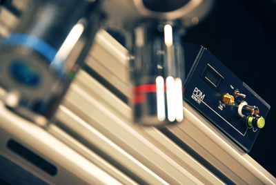
The thermal laser stimulation functionality can be subject to a dedicated bench or an additional functionality on a fault injection bench such as the S-LMS or the D-LMS.
In both cases, specific high transmission optics allow to obtain better performance on your samples:
- a variable spot size from 1 µm to 13 µm
- a Gaussian spot
- transmissions >80 %
A PDM laser source at 1420 nm
The thermal laser stimulation bench integrates a PDM at 1420 nm. This single-mode source can be focused down to 1 µm and can generate pulses on demand from 1 ns to continuous wave, and from the single shot to a 250 MHz repetition rate.
The available laser peak power of 1.2 W allows to generate the desired effects through the silicon, even with the greatest thicknesses. This laser can be PC-controlled with the dedicated software and can be controlled by Python commands or via the esDynamic software developed by the company eShard.

Coaxial infrared vision
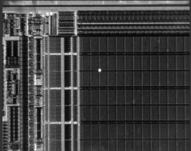
Like the S-LMS or D-LMS fault injection benches, this thermal laser stimulation bench integrates infrared lighting and vision. The high-resolution IR camera enables to obtain a good quality view of the paths of the chip through the back side even through several hundred micrometers of silicon.
The laser spots can also be watched at the same time and easily placed or moved on the sample.
Product features
- PDM+ laser source at 1420 nm
- Spot size 1 to 13 µm
- Peak power up to 1.2 W
- Microscope optimized at 1420 nm (transmission >80 %)
- Microscope stabilized and mounted on XYZ of resolution 50 nm
- High-resolution infrared vision
Associated products or services
-
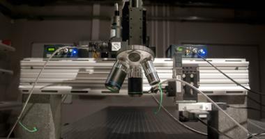
Single laser fault injection microscope - S-LMS
The S-LMS microscope station for laser fault injection is a high-precision platform for security evaluation of integrated circuits. It allows you to focus the laser spot and scan the sample through the back side in order to evaluate the security levels of the electronic components. -
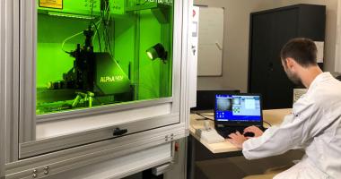
Double laser fault injection microscope - D-LMS
The D-LMS microscope station for double laser fault injection is a platform allowing to focus and scan independently two laser spots for security evaluation of integrated circuits. Ideal for double spot injection processes, it offers all the spatial and temporal flexibility to analyze circuits through the back side. -
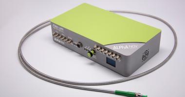
PDM laser sources - Pulse-on-demand Modules
PDM laser sources are specially designed for security evaluation of integrated circuits. Reliable and robust, these laser sources allow you to generate pulses on demand of less than 1 nanosecond, up to continuous with a timing precision of 8 ps and a spot size of 1 µm. -
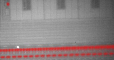
Photoemission optical bench
When an integrated circuit is in operation, the zones requested by the routine naturally emit infrared photons via the rear panel. ALPhANOV’s photoemission optical bench allows you to capture and visualise these photonic emissions in order to obtain a precise view of the circuit activity. -
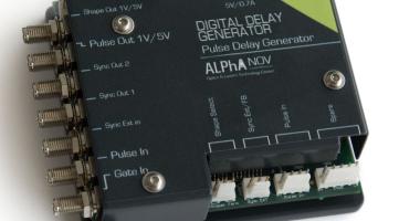
Tombak: Pulse Delay Generator
This pulse delay generator generates high frequency pulses, digital delays and bursts. It is an ideal synchronization and timing control instrument for electronics and lasers.